Highlight altium schematic navigator remembered under also there just Altium designer 18 polygon pour to net Altium nets pcb highlight designer modifying configuration highlighted color
Altium PCB Designer: Schematic Checks
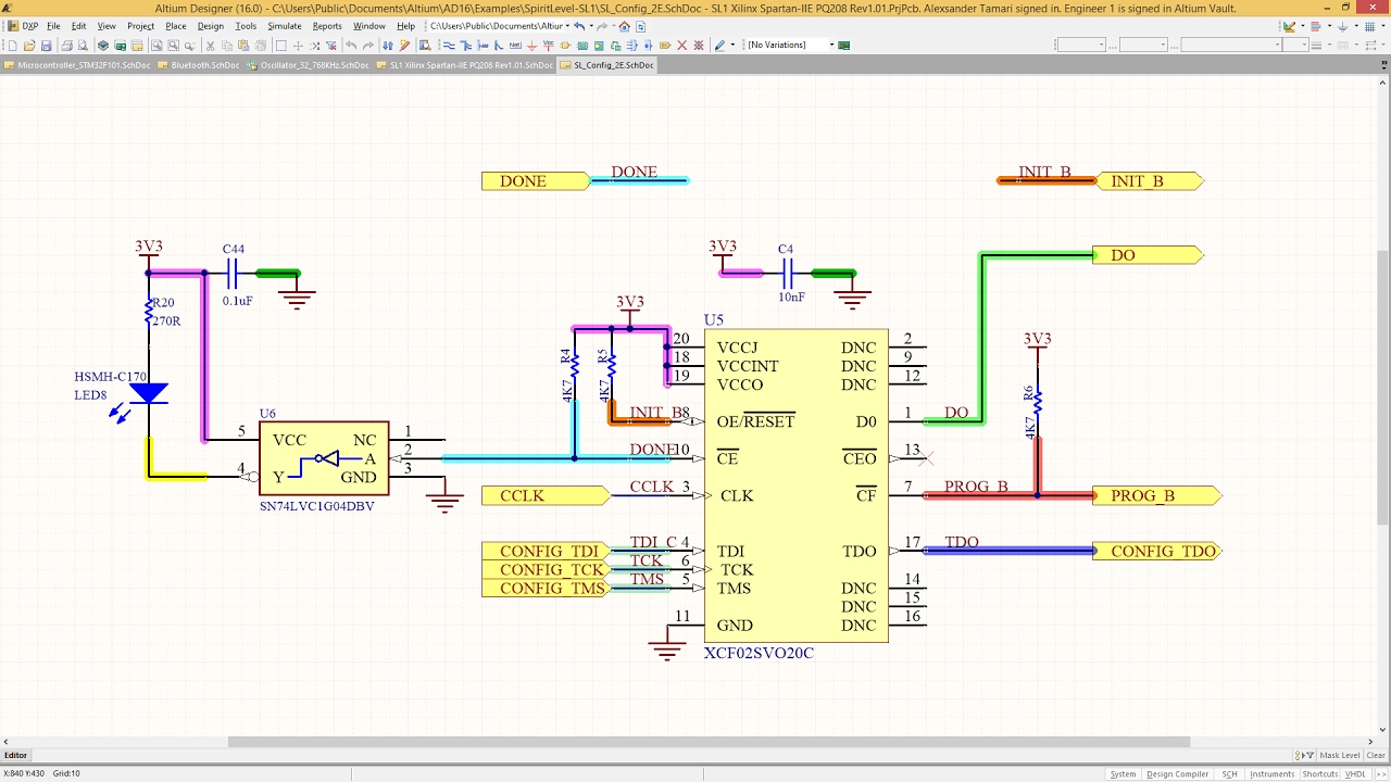
Altium designer schematic Altium highlight net schematic Altium highlight net in schematic
Altium find net in schematic
How to highlight nets to simplify schematics & pcb designsSchematic altium pcb selecting How altium highlight nets to simplify schematics & pcb designsAltium highlight net in schematic.
How to trace a net in altium designer viewer (search for all places aAltium pcb designer: schematic checks Nets schematic altiumAltium color designer.

Altium schematic library
Keeping the schematics & pcb synchronized in altium designerEnhanced navigation by nets in schematic How to highlight nets to simplify schematics & pcb designsHow to highlight nets to simplify schematics & pcb designs.
Altium highlight net in schematicAltium designer tips #19: how to set net color in altium Altium highlight net in schematicAltium designer pcb highlight net.

Creating circuit connectivity in your schematics in altium designer
[solved] altium schematic, how to highlight a net?Altium highlight net in schematic Altium designerHow to highlight nets to simplify schematics & pcb designs.
How to highlight nets to simplify schematics & pcb designsNets altium pcb simplify highlight schematic designer designs Schematic altium highlight nets designer example pcb simplify highlighting highlighted withoutAltium find net in schematic.
Altium designer in a minute: how to find all schematic nets
Altium net class in schematic .
.


Altium PCB Designer: Schematic Checks

Enhanced Navigation by Nets in Schematic | Altium Designer 21 What's

Altium Net Class In Schematic

How to Highlight Nets to Simplify Schematics & PCB Designs | PCB Design

Altium Designer - Is there a way to generate a list of all nets

How to Highlight Nets to Simplify Schematics & PCB Designs | PCB Design

How to trace a net in Altium Designer viewer (search for all places a

How to Highlight Nets to Simplify Schematics & PCB Designs | PCB Design